Backbase die

base die

SK Hynix
2026-08-31 01:28:44

SK Hynix Weighs Intel as Second Foundry for HBM4E Base Dies to Cut Reliance on TSMC

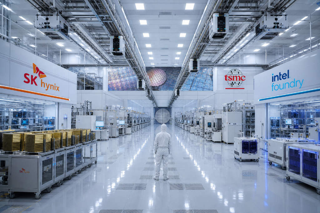
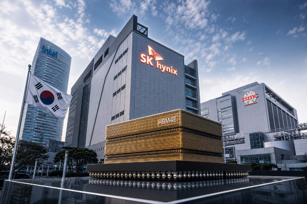
SK Hynix is working to diversify the foundry suppliers for the base dies used in its high-bandwidth memory (HBM) products, according to Citrini analyst Jukan. The company is considering outsourcing part of the base-die production for HBM4E, its seventh-generation high-bandwidth memory, to Intel's foundry. So far, SK Hynix has relied entirely on TSMC for outsourced base-die production. Industry sources said on Aug. 31 that SK Hynix is advancing a plan under which HBM4E base dies could be made by both TSMC and Intel, with the earliest adoption possibly starting with the HBM4E generation. The potential shift is seen as an effort to build a multi-vendor foundry strategy, reducing supply-chain concentration at TSMC and strengthening SK Hynix's pricing power. Market expectations point to higher base-die costs for HBM4E. Since HBM products are mostly covered by long-term supply agreements, SK Hynix cannot quickly pass higher foundry costs on to customers through price increases. Industry observers say that if Intel eventually joins the base-die supply chain, SK Hynix would gain more options in cost competitiveness and supply stability.
20
SK Hynix Weighs Intel as Second Foundry for HBM4E Base Dies to Cut Reliance on TSMC
SK Hynix
2026-08-31 01:26:23

SK Hynix may have Intel make some HBM4E base dies, report says

SK Hynix is considering Intel as a second foundry source for the base dies used in its high-bandwidth memory (HBM) products, according to Citrini analyst Jukan on Aug 31. The company is looking at outsourcing part of the base-die production for HBM4E, the seventh-generation HBM, to Intel's foundry business. So far, SK Hynix has relied entirely on TSMC for outsourced base-die manufacturing. The potential addition of Intel is viewed as part of a push to build a multi-supplier foundry strategy, one that would reduce the supply chain's concentration around TSMC and improve SK Hynix's pricing leverage. Industry sources said SK Hynix is working on a plan where TSMC and Intel jointly produce HBM4E base dies, possibly starting as early as the HBM4E generation. HBM is built by stacking memory chips vertically on a base die. Market expectations point to higher base-die costs for HBM4E. Since HBM products are largely covered by long-term supply agreements, SK Hynix cannot quickly pass higher foundry costs to clients through price increases. Industry observers believe that if Intel eventually joins the base-die supply chain, SK Hynix would gain more options in both cost competitiveness and supply stability.
20
SK Hynix may have Intel make some HBM4E base dies, report says
Samsung
2026-08-28 06:21:45

Samsung Develops 8-Layer HBM4E for Nvidia's Custom NVHBM

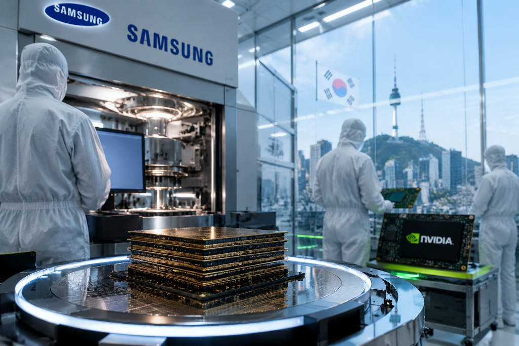
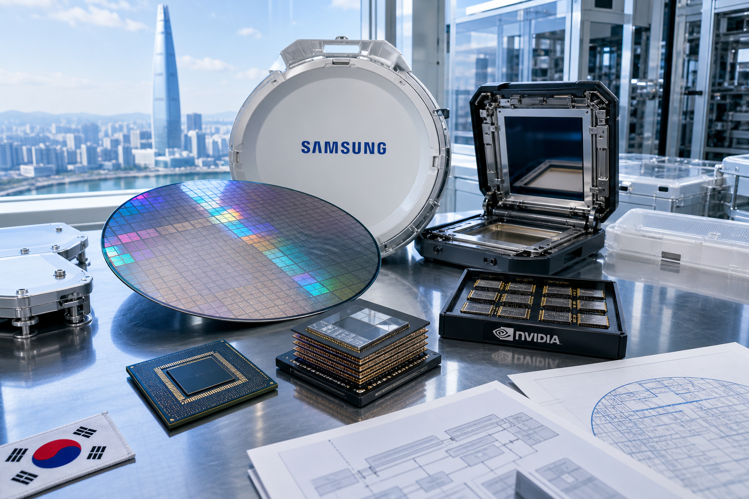
Samsung Electronics is developing an 8-layer HBM4E product at Nvidia's request, according to Korea's Seoul Economic Daily. The chip is intended for Nvidia's custom high-bandwidth memory (NVHBM), and it uses fewer stacked layers than the 12- and 16-layer options Samsung initially prepared. Nvidia's target speed for the memory is 17–18 Gbps, about 20% faster than the 14.4 Gbps seen in Samsung's early HBM4E samples. The simplified layering is expected to reduce manufacturing difficulty in wafer thinning, precision stacking, and packaging, improving yield and supply potential. NVHBM could first appear on Nvidia's upcoming Rubin Ultra AI GPU, which is slated for next year; the platform plans to scale GPU interconnect from 72 to up to 576 units to offset lower per-GPU memory capacity. Samsung, which designs and produces DRAM, logic chips, and base dies, says it can provide one-stop custom HBM services. Industry observers note that Samsung has already shown strong transfer speeds with HBM4, and its capabilities may gain more attention as Nvidia shifts its focus from high stacking to high-speed transmission.

110
Samsung Develops 8-Layer HBM4E for Nvidia's Custom NVHBM
Samsung Elect
2026-08-28 06:27:38

Samsung develops 8-layer HBM4E for Nvidia as it targets a core NVHBM supply role

Samsung Electronics is developing an 8-layer HBM4E, or seventh-generation high-bandwidth memory, product tailored to Nvidia’s requirements, according to a report by Seoul Economic cited by ChainCatcher. The effort is aimed at securing a core partner position in the supply chain for Nvidia’s custom NVHBM memory. The report says the new design lowers stack height compared with Samsung’s earlier 12-layer and 16-layer plans, while targeting speeds of 17-18Gbps, about 20% above the 14.4Gbps level of Samsung’s initial HBM4E samples. Nvidia is said to be planning the memory for NVHBM built around its publicly disclosed NVLink-optimized specifications. Seoul Economic also said the 8-layer approach runs against the usual HBM strategy of increasing capacity through more stacked layers, but could ease backend process complexity and reduce yield pressure, making it easier to expand supply. The report added that Nvidia may use that design choice to address memory shortages. NVHBM could begin shipping with Rubin Ultra, Nvidia’s next-generation AI GPU expected next year, which would expand GPU-to-GPU interconnect scale from 72 to as many as 576. In the custom HBM market, the report said Samsung may hold an edge over SK hynix and Micron because NVHBM requires both DRAM capability and logic-die-based base die design and manufacturing.

110
Samsung develops 8-layer HBM4E for Nvidia as it targets a core NVHBM supply role
NVIDIA
2026-08-27 00:43:29

NVIDIA Unveils NVHBM as AWS Lines Up Trainium4 Support and a Major GPU Deal

NVIDIA has introduced NVHBM, a new custom high-bandwidth memory technology, and folded it into its NVLink Fusion ecosystem as AI infrastructure demands shift beyond raw compute toward tighter coordination across processors, memory, interconnects, and cooling. AWS chip unit Annapurna Labs is the first partner to adopt the technology and said its next-generation in-house Trainium4 chip will support both NVLink Fusion and NVHBM. The announcement came alongside a separate commercial commitment: Amazon confirmed plans to buy up to 2 million next-generation high-end GPUs from NVIDIA between 2027 and 2028, covering Blackwell Ultra, Rubin, and Rubin Ultra. According to ABMedia, the arrangement reflects a changing relationship between hyperscalers and NVIDIA, where internal chip development and external GPU procurement now sit side by side rather than in direct opposition. ABMedia said NVHBM moves the memory controller into the base die of a 3D HBM stack, freeing die space on the XPU for more compute cores or cache. The report cited gains of up to 30% more memory bandwidth, about 15% lower HBM power consumption, and up to 25% more chip area released for compute. NVIDIA is also pushing the design toward a standardized specification across suppliers including SK hynix, Samsung, and Micron.

170
NVIDIA Unveils NVHBM as AWS Lines Up Trainium4 Support and a Major GPU Deal
Nvidia
2026-08-26 21:20:48

Nvidia launches NVHBM and partners with AWS unit Annapurna Labs on AI infrastructure

Nvidia said it has expanded its NVLink Fusion platform with NVHBM, a next-generation high-bandwidth memory technology aimed at improving AI infrastructure efficiency. According to the company’s blog, NVHBM integrates the memory controller into the HBM base die. Compared with standard HBM4E, the design can deliver up to 30% more memory bandwidth, cut HBM power consumption by 15%, and free up as much as 25% of die area for XPU compute chips. Amazon’s Annapurna Labs will be the first partner to adopt NVHBM as part of a broader collaboration with Nvidia around NVLink Fusion. The two companies said they will use the technology together with NVLink scale-up architecture to improve the performance and efficiency of AI workloads. Nvidia also said NVHBM will be offered as a standard implementation and validated by multiple memory suppliers. The company said the approach is intended to help hyperscalers and AI-native companies deploy semi-custom AI infrastructure faster and with lower risk.

150
Nvidia launches NVHBM and partners with AWS unit Annapurna Labs on AI infrastructure
HBM
2026-08-25 01:13:19

HBM Splits Into Diverging Paths as Samsung Pushes zHBM and SK Hynix Targets Taller Stacks

High Bandwidth Memory is no longer being framed as a standalone memory problem. At Hot Chips 2026, Samsung and SK Hynix both argued that GPUs, memory, foundry processes and packaging now have to be designed as one system, but the two companies outlined sharply different routes. Samsung is trying to turn the HBM base die from a passive bridge into an active logic layer, moving the memory controller off the GPU, adding memory expansion and selective compute to the base die, and ultimately aiming for zHBM, a structure that vertically stacks DRAM directly on top of compute silicon. Samsung said that approach could free up 5% to 10% of GPU area, lift performance by 10% to 20%, cut DRAM power by about 70%, and deliver more than 2.3x the bandwidth of HBM4E. SK Hynix, by contrast, is concentrating on higher stack counts and the thermal and warpage penalties that come with them. The company said 12-high HBM4 is in production and 16-high parts are in customer validation, while hybrid bonding remains in R&D for 20-high and above. It also presented iHBM, a thermal path built into the hottest region of the stack. Micron took a third angle, arguing that the AI memory wall is widening as accelerator compute rises faster than attached-memory bandwidth, forcing increasingly difficult trade-offs across bandwidth, capacity, packaging complexity, heat and reliability.

630
HBM Splits Into Diverging Paths as Samsung Pushes zHBM and SK Hynix Targets Taller Stacks
Samsung Elect
2026-08-14 08:00:08

Samsung weighs shifting NRD-K Line 2 to foundry output for cHBM and HBM5 base dies

Samsung Electronics is considering repurposing Line 2 at its next-generation NRD-K semiconductor R&D complex in Giheung from a research line into a foundry production line, according to analyst Jukan, who cited South Korean media on Aug. 14. The move is aimed at expanding 2nm capacity for base chips used in high-bandwidth memory, with a focus on custom HBM and HBM5 demand from customers including Nvidia. The line is expected to begin operations in the second half of 2028 and would run under a Send Fab model, receiving wafers from other mass-production lines and handling only specific process steps as an auxiliary foundry facility. NRD-K, built with an investment of about 20 trillion won, is Samsung’s most advanced combined R&D complex and includes three planned lines. Line 1 was completed at the end of 2024. The report said Samsung is positioning early for a surge in HBM demand tied to AI infrastructure. By applying 2nm technology first to custom HBM and HBM5, the company is seeking to stay competitive on performance in advanced packaging base chips. Industry views cited in the report said Line 2 is relatively small and well suited to the Send Fab role, though its final use could still change with market conditions and equipment purchase orders have not yet been formally issued.

670
Samsung weighs shifting NRD-K Line 2 to foundry output for cHBM and HBM5 base dies